Topological insulators form optical cavities.
Holograms reproduce both the intensity and phase of recorded light; therefore, unlike traditional photographs, holograms have the potential to faithfully reproduce a full three-dimensional scene. In order for this to be possible, holograms generally need to be thick, thereby limiting potential applications. Now, a team led by Min Gu at the Royal Melbourne Institute of Technology (RMIT) in Australia has thinned holograms down to 25 nm, paving the way for integrated flat optoelectronic devices.
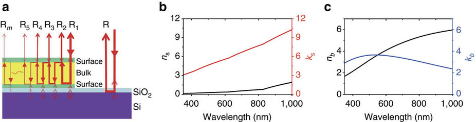
Holograms need to impart a phase delay on light. One way to that goal is metasurface holograms based on scattering, which although thin, still need to be a couple of hundred nanometers thick. Here, researchers realized an alternative route utilizing an unusual physical property of a topological insulator (TI) to form an optical cavity-based hologram. TIs behave as a metal on surfaces and a dielectric on the inside. Therefore a film is similar to two silvered mirrors sandwiching a piece of glass – light can be temporarily trapped in this cavity, bouncing back-and-forth, and acquiring phase with each pass.
After depositing the TI (Sb2Te3) on a silicon substrate, direct laser writing was used to write a binary hologram. In the regions where the TI remained, incident light was phase-shifted exactly as planned. The bare regions had an unavoidable, but expected, layer of glass coating the silicon substrate which generated a different, smaller phase shift. Together, complex holograms were demonstrated with several different colors.
The interplay between hologram performance and thickness was further studied. While holograms as thin as 25 nm were demonstrated, hologram quality improves as the thickness is increased since a larger phase shift can be introduced. Still, a near-ideal balance was found for only 60 nm thick films and continued materials develop holds promise to further thin the holograms. The combined thin form and scalable fabrication will enable the integration of these holograms into the next generation of thin optoelectronics, spanning imaging, data storage, and security applications.
Reference & Image Credit
Yue, Z. et al. Nanometric holograms based on a topological insulator material. Nature Communications http://dx.doi.org/10.1038/ncomms15354 (2017)
More about phase.

Leave a comment